Atomic Force Microscope (AFM)

Brand : Park Systems
Model : NX-10
Scan range : 15μm (optional 30 μm), Resolution – 0.015 nm, Position detector noise – 0.03 nm (bandwidth: 1 kHz), Resonant frequency> 9 kHz (typically 10.5 kHz)

AFM is a type of scanning probe microscopy (SPM), with demonstrated resolution on the order of fractions of a nanometer, more than 1000 times better than the optical diffraction limit. The information is gathered by “feeling” or “touching” the surface with a mechanical probe. Piezoelectric elements that facilitate tiny but accurate and precise movements on (electronic) command enable precise scanning. The AFM consists of a cantilever with a sharp tip (probe) at its end that is used to scan the specimen surface. The cantilever is typically silicon or silicon nitride with a tip radius of curvature on the order of nanometers.

The AFM has been applied to problems in a wide range of disciplines of the natural sciences, including solid-state physics, semiconductor science and technology, molecular engineering, polymer chemistry and physics, surface chemistry, molecular biology, cell biology, and medicine. Applications in the field of solid state physics include (a) the identification of atoms at a surface, (b) the evaluation of interactions between a specific atom and its neighboring atoms, and (c) the study of changes in physical properties arising from changes in an atomic arrangement through atomic manipulation.

In cellular biology, AFM can be used to distinguish cancer cells and normal cells based on a hardness of cells, and to evaluate interactions between a specific cell and its neighboring cells in a competitive culture system. AFM can also be used to indent cells, to study how they regulate the stiffness or shape of the cell membrane or wall.

Category:

Biology and Biotechnology
Proteins, DNA, viruses, bacteriums, tissues

Materials Science
Surface morphology, local piezoelectric properties, local adhesion properties, local tribological properties, surface potential

Magnetic Materials
Magnetic domain structure visualization, observation of magnetization reversal processes that depend on external magnetic field, observation of magnetization reversal processes under different temperatures

Semiconductors, Electric Measurements
Wafers and other structures morphology, local surface potential and capacitance measurements, electric domain structure imaging, determination of heterojunction bounds and semiconductor regions with different doping levels, failure analysis (localization of conductor line failure and leakage in dielectric layers)

Polymers and Thin Organic Films
Spherulites and dendrites, polymer monocrystals, polymer nanoparticles, LB-films, thin organic films

Data Storage Devices and Medias
CD, DVD disks, storages for terabit memories with thermomechanical, electric and other types of recording

Nanomaterials
Nanopowders, nanocomposites, nanoporous materials

Nanostructures
Fullerenes, nanotubes, nanofilaments, nanocapsules

Nanoelectronics
Quantum dots, nanowires, quantum structures

Nanomachining
AFM lithography: force (ac and dc), current (Local anodic oxidation), STM lithography 

All enquiries please contact:
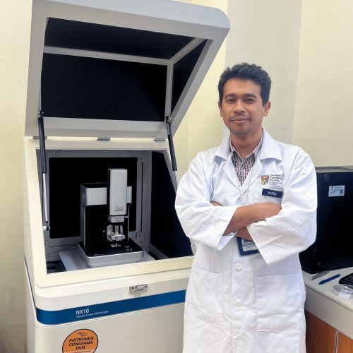
MUHAMMAD NAZRUL ZAHARI

Diploma (UiTM) Industrial Chemistry

Email: nazrul87@ukm.edu.my
Contact Number: 03-8911 8512

Location: Level 3, i-CRIM Centralised Lab, Centre for Natural and Physical Laboratory Management UKM (ALAF-UKM), Research Complex UKM